[an error occurred while processing this directive]
English

[an error occurred while processing this directive]

0512-67162577
0512-67504261

Scan QR code to follow WeChat public account

School‑enterprise cooperation|Visiting an alumni company — Sunmoon New Semiconductor (Suzhou), gaining in‑depth understanding of chip manufacturing processes
announcer:MBA Education Center release time:2026-03-09views:10
In the deep integration of a new round of technological revolution and industrial transformation, the semiconductor industry, as the core cornerstone of modern industry, sees every manufacturing link embodying the pinnacle of human wisdom. From design blueprints to final products, the "birth" journey of a chip is filled with collisions of technology and craftsmanship.
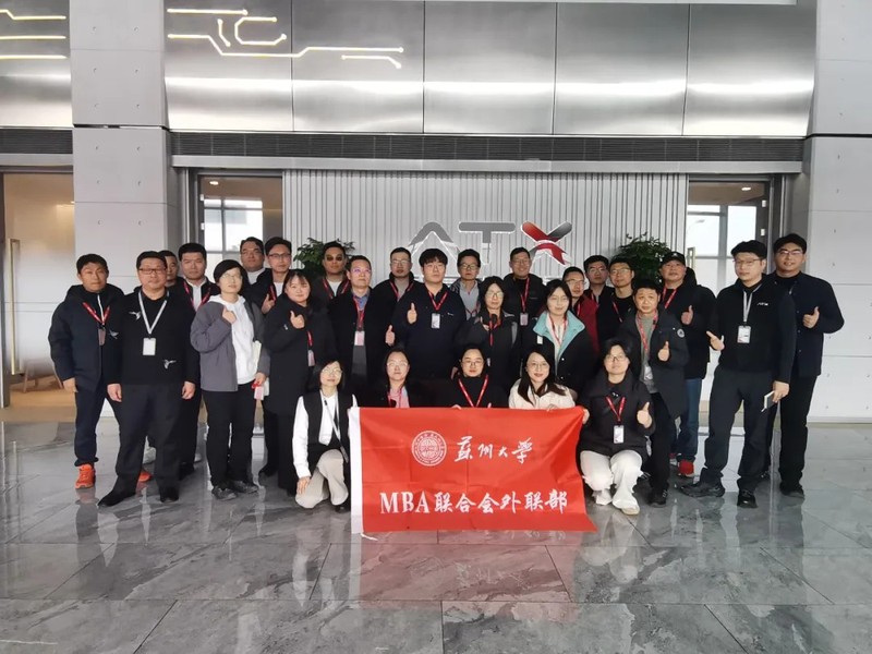
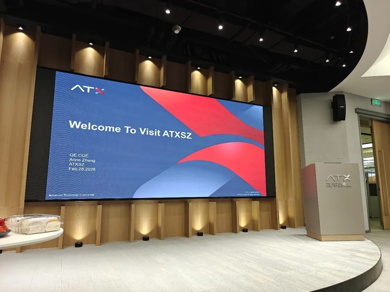
On February 28, 2026, with the afterglow of the Lunar Year of the Horse’s Spring Festival still lingering, Suzhou Industrial Park was already full of the vigor of post‑holiday restart. The warm spring sun dispelled the winter chill and reflected the passionate enthusiasm of Suzhou University MBA students exploring "hard tech." Riding the momentum of the new spring and renewed beginnings, the Suzhou University MBA Association External Relations Department organized students to visit an industry benchmark enterprise located in Suzhou Industrial Park — Sunmoon New Semiconductor (Suzhou) Co., Ltd., embarking on an in‑depth exploration of chip packaging and testing. Observing up close this packaging and testing giant hidden behind the scenes, they decoded how chips are endowed with a powerful "body" and the "bridge" of their soul.
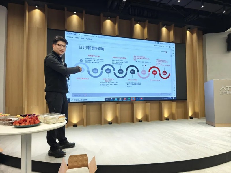
Sunmoon New Semiconductor (Suzhou) Co., Ltd. was founded in 2001 and is located in Suzhou Industrial Park, Jiangsu Province, which has topped the list of "China’s Most Competitive Development Zones" for consecutive years. As a high‑tech enterprise with deep technological accumulation and sustained innovation vitality, Sunmoon New has always invested in the R&D of advanced semiconductor process technologies with a forward‑looking vision.
The company has a high‑quality R&D team that continuously focuses on breakthroughs in advanced technologies and processes, committed to meeting customers’ dual needs for enhanced product functionality and cost reduction. With solid R&D strength, Sunmoon New has accumulated multiple technology patents, building powerful and reliable solutions for cutting‑edge application fields such as connected vehicles, network security, portable and wearable applications, the Internet of Things, and 5G networks.
From wafer probing, die test program development to substrate design, Sunmoon New provides full‑process services covering integrated circuit and semiconductor device R&D, packaging, and testing. The company’s annual packaging and testing chip capacity has exceeded 800 million units, and its MEMS packaging technology has been selected as a national‑level innovation project, making it one of the representative enterprises in the Yangtze River Delta region’s semiconductor packaging and testing field.
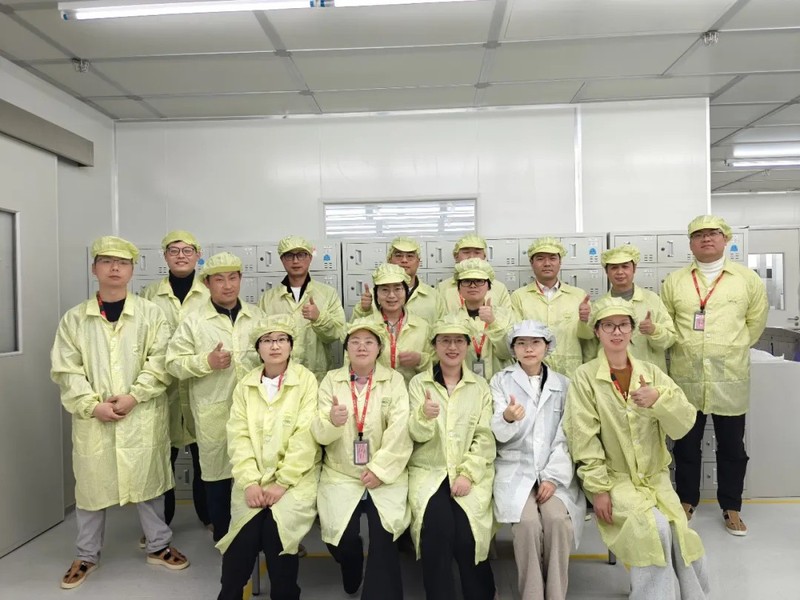
This visit was not a simple corporate tour but more like a vivid "industry dissection class." Guided by company leaders, students put on professional anti‑static suits and entered the laboratory area to witness the backend inspection processes of chip packaging and testing firsthand.
Unlike traditional manufacturing, semiconductor packaging and testing is a typical combination of technology intensity and capital intensity. In the laboratory session, students closely observed demonstrations of core chip packaging and testing processes. Company technicians, using the experimental equipment, explained in detail the core technical principles from grinding and dicing, wire bonding processes to molding and encapsulation. Especially when presenting experimental data comparisons of advanced processes such as vacuum reflow soldering and mass transfer, students, through microscope observation and real‑time parameter analysis, deeply felt the true meaning of "engineering wisdom lies in the details, and yield control depends on the whole picture."
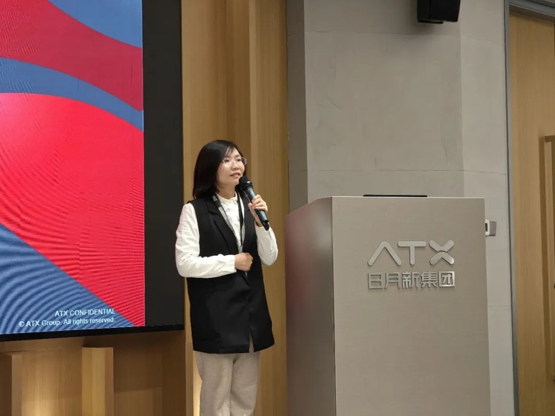
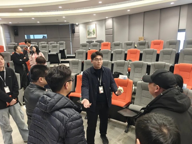
After the tour, company leaders held an in‑depth discussion with Suzhou University MBA faculty and students. Unlike purely technical briefings, the discussion focused more on industry trends, corporate strategy and talent development.
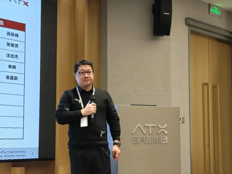
This Suzhou University MBA school‑enterprise visit received great attention and careful guidance from Senior Director Ren Linfeng of the company’s Quality Department, and strong support from CQE Manager Gao Junfeng. The event invited Packaging Sales Manager Zhu Feng and Senior Manager of the Technical Department Shen Zhijie to attend and exchange ideas, engaging students in in‑depth discussions on topics such as the semiconductor industry landscape, corporate cost control, and balancing technological innovation. Laboratory Sales Manager Xin Yun was on a business trip and unable to attend, and specially appointed engineer Yuan Jiawei to participate and share the latest technology dynamics in the packaging and testing field with the students.
Facing students’ questions about China’s semiconductor ecosystem position, advanced packaging technology trends, and the value of versatile management talent in manufacturing, company representatives, drawing on Sunmoon New’s philosophy of "upholding integrity, pragmatic work, and long‑term effort," shared how the company builds its core competitiveness amid intense global competition through continuous technology R&D and improving the coverage of intelligent manufacturing systems. The company also specifically mentioned that Sunmoon New provides university graduates with solid training and promotion mechanisms, encouraging young people to work on the front lines of the industry and grow into versatile talents who understand both technology and management.
As an alumni enterprise of Suzhou University, Sunmoon New Semiconductor has given strong support to school‑enterprise exchanges. With extensive support from all parties at the company, this event was coordinated and organized throughout by MBA student Zhang Junfang; thanks are also due to the External Relations Department of the Suzhou University MBA Association for meticulous preparation and to all students for their active participation, making the event a complete success.
This visit not only allowed students to see real industry scenes beyond textbooks, but also helped them deeply understand the business decision‑making logic behind chip manufacturing processes.
A good school‑enterprise visit is not a superficial tour, but a way to see the underlying logic of technological iteration and industrial development through precise equipment and rigorous processes.
Thanks to Sunmoon New Semiconductor (Suzhou) Co., Ltd. for their warm reception and selfless sharing. In the future, the Suzhou University MBA Association will continue to connect with more outstanding alumni enterprises, leading students to the front lines of industry to draw rich nourishment for their professional careers from real commercial soil.
